登录后查看价格
收藏

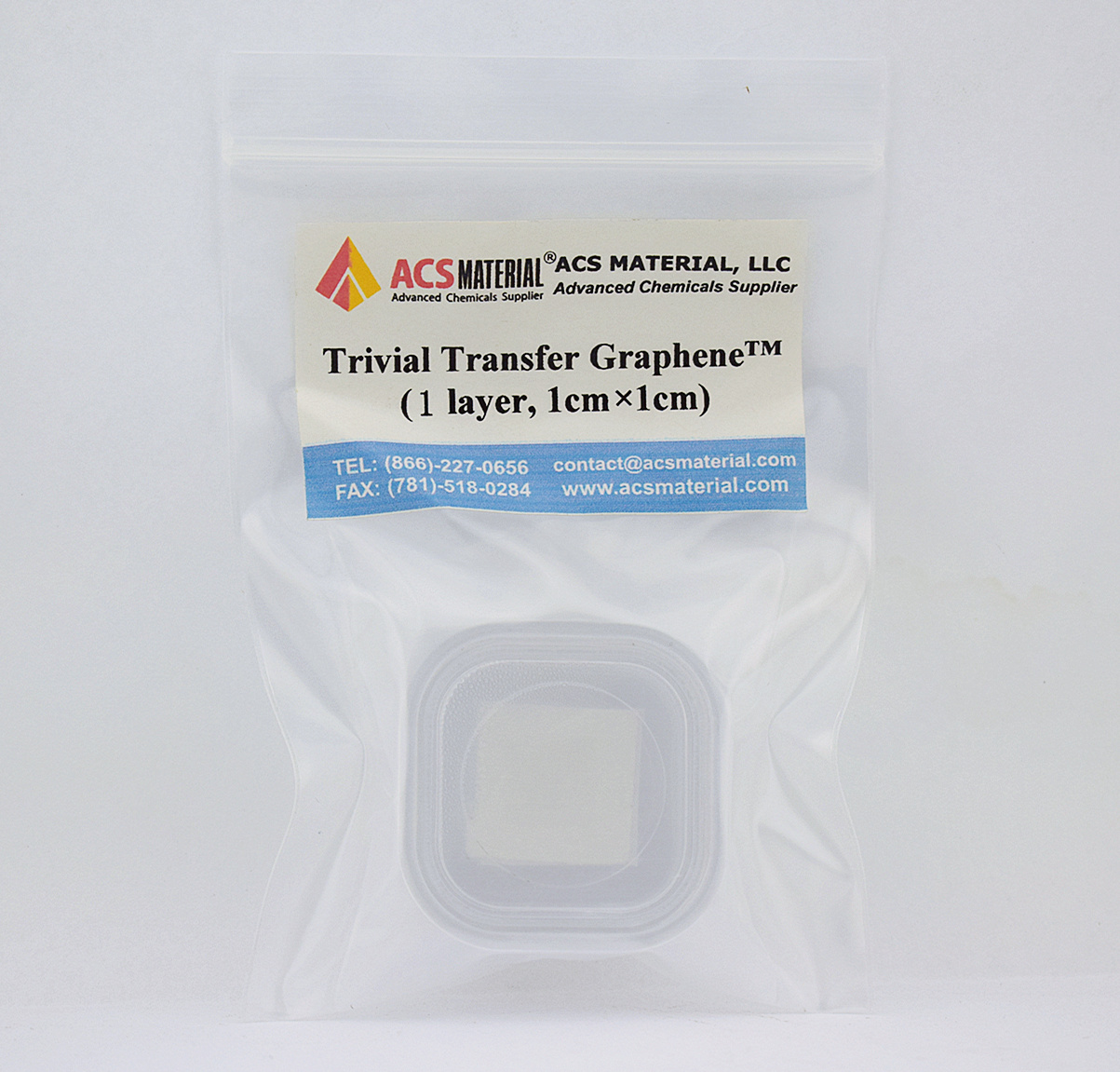
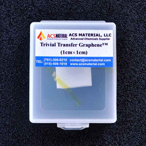
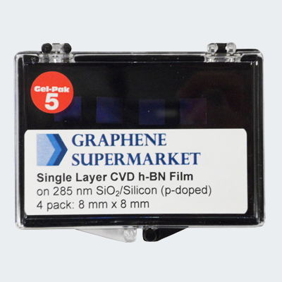
GS 二氧化硅基底单层氮化硼薄膜
货号:100175 编号:XF059
CAS号:7440-44-0 规格:1盒 4片 8mmx8mm
包装:1盒 保质期:0天
保存条件:常温干燥避光密封
暂无技术资料
可选
请选择规格参数

包装:每盒4片 面积:8mm*8mm单片 基底:二氧化硅基底
Single Layer CVD hexagonal Boron Nitride Film on 285 nm SiO2/Si substrates (p-doped), 8 mm x 8 mm: 4 pack
Properties of BN film
95% coverage
High Crystalline Quality
The Raman spectrum should peak at ~1369cm-1

The Raman Signal of BN on SiO2/Si is very weak. To characterize h-BN on SiO2/Si using Raman spectroscopy, you need to use a blue or high power laser and the signal may not be detectable on certain commercial systems. For more information regarding Raman spectroscopy and characterization of h-BN on SiO2/Si, refer to the following paper: Hunting for Monolayer Boron Nitride: Optical and Raman Signatures .
The h-BN film is grown via CVD onto copper foil, then transferred to the SiO2/Si substrate. To see characterizations of the film before transfer, see our related product, h-BN on Copper Foil.
Applications:
BN on SiO2/Si wafers are ideal for creating graphene/BN interfaces, allowing the graphene to be precisely gated, increasing mobility, and reducing scattering. h-BN is appealing as a substrate for graphene-based electronics because its surface is atomically smooth, it is free of dangling bonds, and has an analogous structure to graphene. Using our h-BN on SiO2/Si wafers in conjunction with graphene, we encourage you to explore graphene heterostructures for transistor applications.

江浙沪皖用户邮费为10元,其他地区用户邮费为20, 国际运费请咨询sales@xfnano.com。购买满 500.0 元免运费。如果库存显示为0, 请电话或邮件和销售确认,免费热线电话:400 025 3200邮件:sale@xfnano.com 感谢您的支持!